PB430.003 /03-01-94 |0| Copyright 1991-1994 Packard Bell Electronics
PB430/440/440T UPGRADE INFORMATION
NOTE: Only authorized service personnel should upgrade the system. Anyone who wants to upgrade the system herself/himself should know about the dangers of ESD (Electro-Static Discharge) and the necessary precautions. Unknowingly zapping the components of the computer will void the warranty.
1. MEMORY
NOTES:
| SMT | SIMM1 | SIMM2 | Total | Base | Ext. |
| 4MB | None | None | 4MB | 640 | 3200 |
| 4MB | 4MB | None | 8MB | 640 | 7296 |
| 4MB | None | 4MB | 8MB | 640 | 7296 |
| 4MB | 4MB | 4MB | 12MB | 640 | 11392 |
| 4MB | 8MB | None | 12MB | 640 | 11392 |
| 4MB | 8MB | 4MB | 16MB | 640 | 16488 |
| 4MB | 16MB | None | 20MB | 640 | 19584 |
| 4MB | None | 16MB | 20MB | 640 | 19584 |
| 4MB | 16MB | 4MB | 24MB | 640 | 23680 |
| 4MB | 4MB | 16MB | 24MB | 640 | 23680 |
| 4MB | 8MB | 16MB | 28MB | 640 | 27776 |
| 4MB | 16MB | 16MB | 36MB | 640 | 35968 |
| 4MB | 32MB | None | 36MB | 640 | 35968 |
| 4MB | 32MB | 4MB | 40MB | 640 | 40064 |
| 4MB | 32MB | 16MB | 52MB | 640 | 52352 |
| *4MB | 32MB | 32MB | 64MB | 640 | 64640 |
*NOTE: When two 32 MB SIMMS are installed, the SMT memory needs to be disabled.
2. MATH CO-PROCESSOR-CPU UPGRADE
2. MATH CO-PROCESSOR
NOTE:
1. Intel has changed the designations of the 80486 OverDrive processors. In
the table below, the original designations are in parenthesis.
2. To open the upgrade processor socket, pull the tab/lever straight up from the side of the socket (closest to the back of the motherboard) and pull towards the front.
3. This motherboard will accommodate the P24T processor when it becomes available.
The following jumpers are used:
| UPGRADE SOCKET | J23 1-2 | J25 1-2 | J26 1-2 | J34 1-2 | J34 3-4 | J34 5-6 | J40 1-2 | J40 3-4 | J40 5-6 |
| 486SX25 | Out | In | In | Out | Out | In | Out | In | Out |
| 487SX25 | Out | In | In | Out | In | Out | In | Out | In |
| DX2ODP50 (ODP48625) DX4ODP75 or P24T |
Out | In | In | Out | In | Out | In | Out | In |
| DX2ODPR50 (ODPR48625) or DX4ODPR75 |
Out | In | In | In | Out | In | In | Out | In |
| 486DX25 | Out | In | In | In | Out | In | In | Out | In |
| 486SX33 | Out | In | Out | Out | Out | In | Out | In | Out |
| 487SX33 | Out | In | Out | Out | In | Out | In | Out | In |
| 486SX2-50 | Out | In | In | In | Out | In | In | Out | In |
| DX2ODP66 (ODP48633) or DX4ODP100 |
Out | In | Out | Out | In | Out | In | Out | In |
| DX2ODPR66 (ODPR48633) or DX4ODPR100 |
Out | In | Out | In | Out | In | In | Out | In |
| 486DX33 | Out | In | Out | In | Out | In | In | Out | In |
| 486SX2-50 | Out | In | In | In | Out | In | In | Out | In |
| 486DX2-50 | Out | In | In | In | Out | In | In | Out | In |
| 486DX2-66 | Out | In | Out | In | Out | In | In | Out | In |
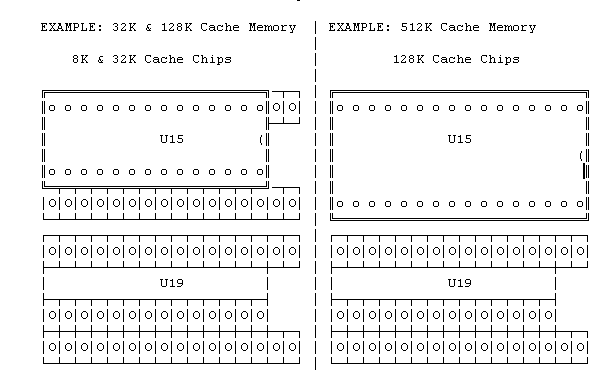
3. CACHE
JUMPER SETTINGS
| JUMPER | 32K | 128K | 512K |
| J30 (Jcach) | Open | Closed | Closed |
| J31 (Jcach) | 1-2 | 2-3 | 2-3 |
| J32 (Jcach) | 1-2 | 2-3 | 2-3 |
| J33 (Jcach) | 1-2 | 1-2 | 2-3 |
SURFACE MOUNT CONFIGURATIONS
NOTE:
| CACHE CHIP TYPE | 32K | 128K | 512K |
| Tag/DB SRAM (U35) | One 8Kx8 | One 32Kx8 | One 128Kx8 |
| Cache (U15,19,24,30) | Four 8Kx8 | Four 32Kx8 | Four 128Kx8 |
BLOW-UP OF CACHE SOCKETS
NOTES:
4. VIDEO MEMORY NOTES:
1. Check with customer service for the availability of the video upgrade memory
2. The DRAM ZIP used in this motherboard is NOT the same chip used for the
PB410/420/420T systems.
3. A VESA driver is not needed for Cirrus video. VESA software compatibility
is built into the PB430/440/440T BIOS.
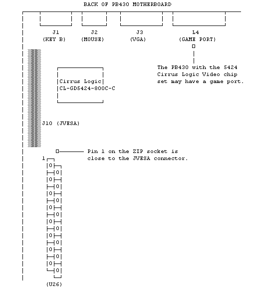
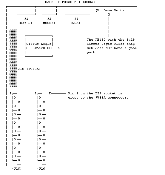
There are two versions of the PB430 motherboard. The main difference between the two motherboards is in the Video Chip set. One has the Cirrus Logic 5424 Video Chip Set, and the other has the Cirrus Logic 5428 Video Chip Set.
Video memory on the PB430 with a CL 5424 chip is upgradeable to 1 MB by installing a 256k x 16 Fast Page Mode DRAM ZIP (Symmetrical, CAS Line) at location U26. The PB430 with a CL 5428 chip is upgradeable to 2 MB of video memory by adding two such DRAM ZIPs.
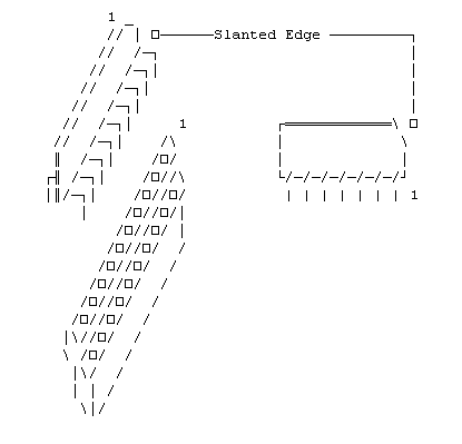
The part number for one such ZIP is: MT4C16257Z
Pin 1 on the DRAM ZIP is on the "slanted" side of the chip, as
shown below:
A. PB430 WITH CIRRUS LOGIC 5424 VIDEO CHIP SET
Pin 1 on the ZIP socket on the PB430 motherboard, is located towards the back left side of
the motherboard, close to the JVESA connector:
B. PB430 WITH CIRRUS LOGIC 5428 VIDEO CHIP SET
Pin 1 on the ZIP socket on the PB430 motherboard, is located towards the back left side of
the motherboard, close to the JVESA connector:
5. SPEAKER Use a standard 8 ohm, 1/2 watt
computer speaker. Move the cap on jumper J39 to pins 2 and 3, and attach the speaker
to connector J39, pins 1 and 4.
6. BATTERY Use a 3.6 Volt lithium
battery. Remove the shorting cap on jumper J24. Then attach the battery to
connector J28, positive to pin 1, negative to pin 4.
Packard-Bell is a trademark of Packard Bell/NEC. This author and the service provider are not affiliated with Packard-Bell/NEC in any way